STM32F405 Development Board
with Switching Power Supply
A compact 4-layer development board built around the STM32F405RGT6 microcontroller, featuring an on-board 12V→3.3V synchronous buck converter, USB OTG FS, SWD debug interface, I²C, UART, and reverse-polarity protection. Designed from scratch in KiCad as a learning exercise in mixed-signal PCB design.
Board Renders
3D renders generated directly from KiCad showing the complete populated board from multiple angles.
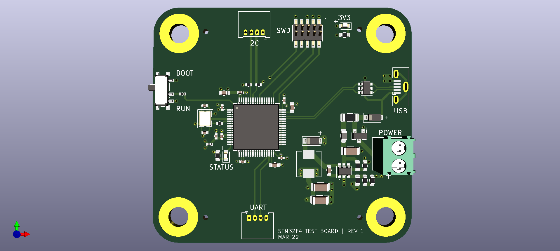
Top view — component placement overview
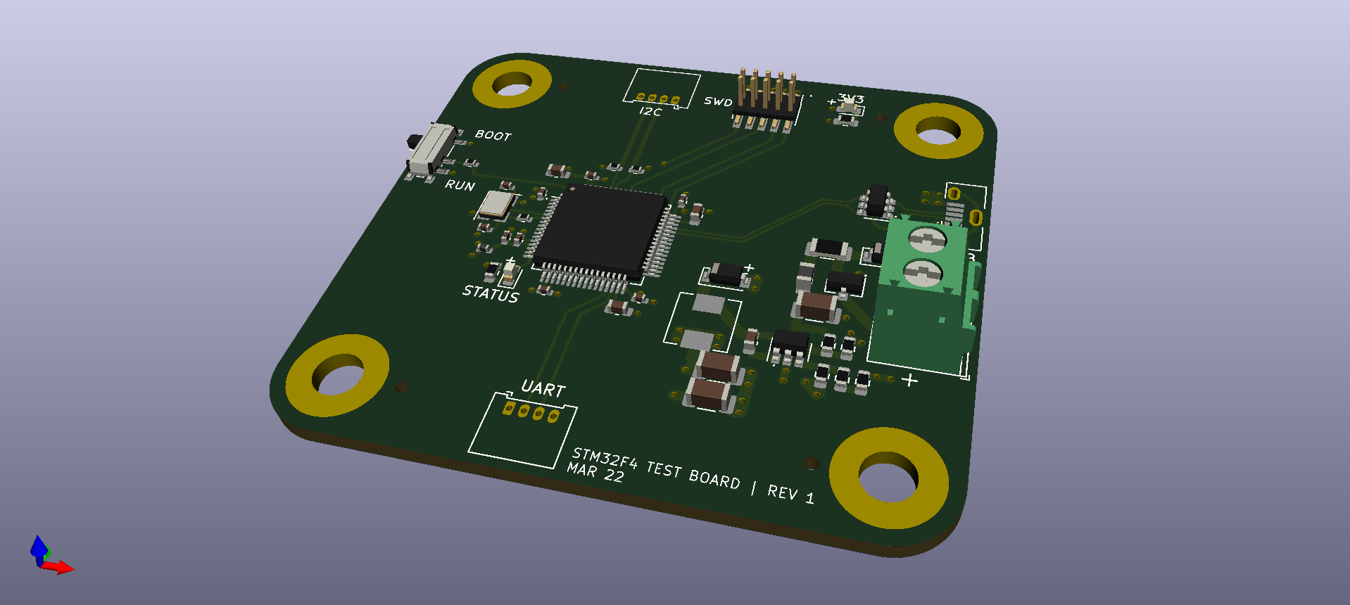
Isometric view — power section right, MCU centre-left
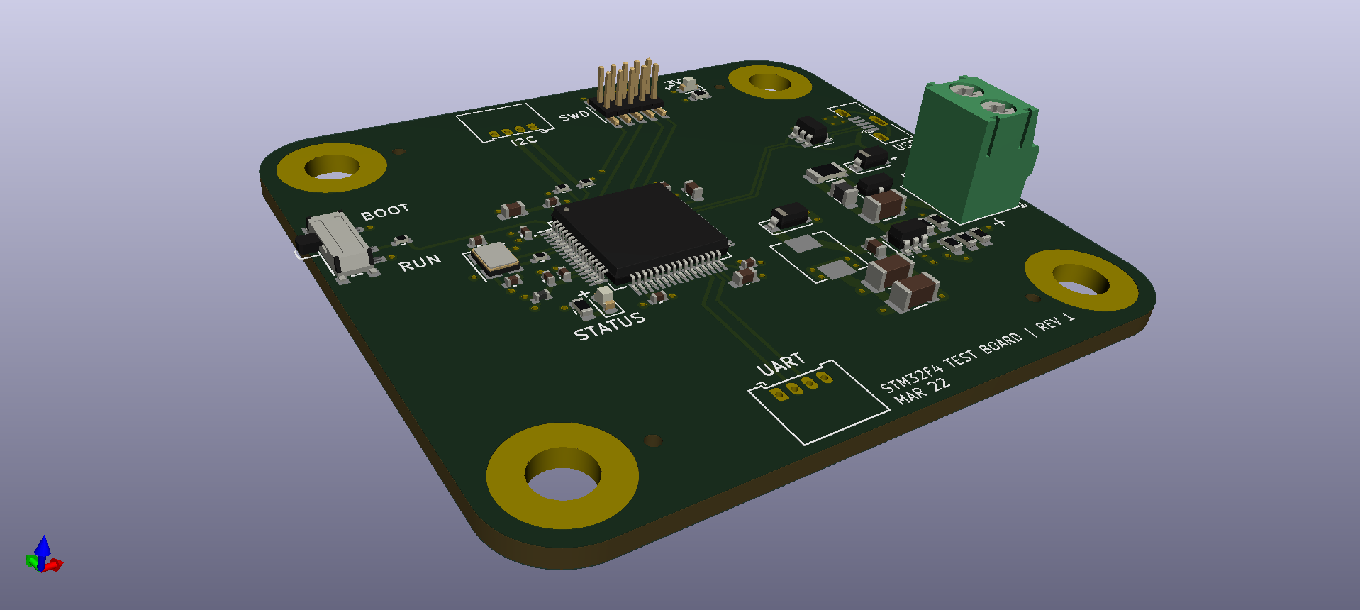
Side angle — showing connector height and board profile
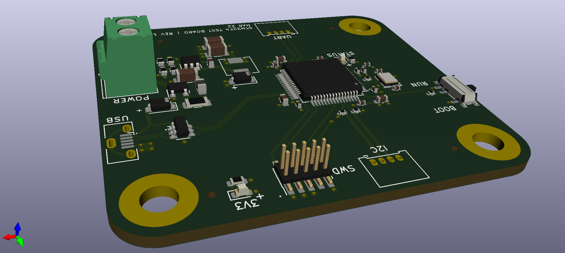
Bottom view — showing SWD, I²C headers and component overlay
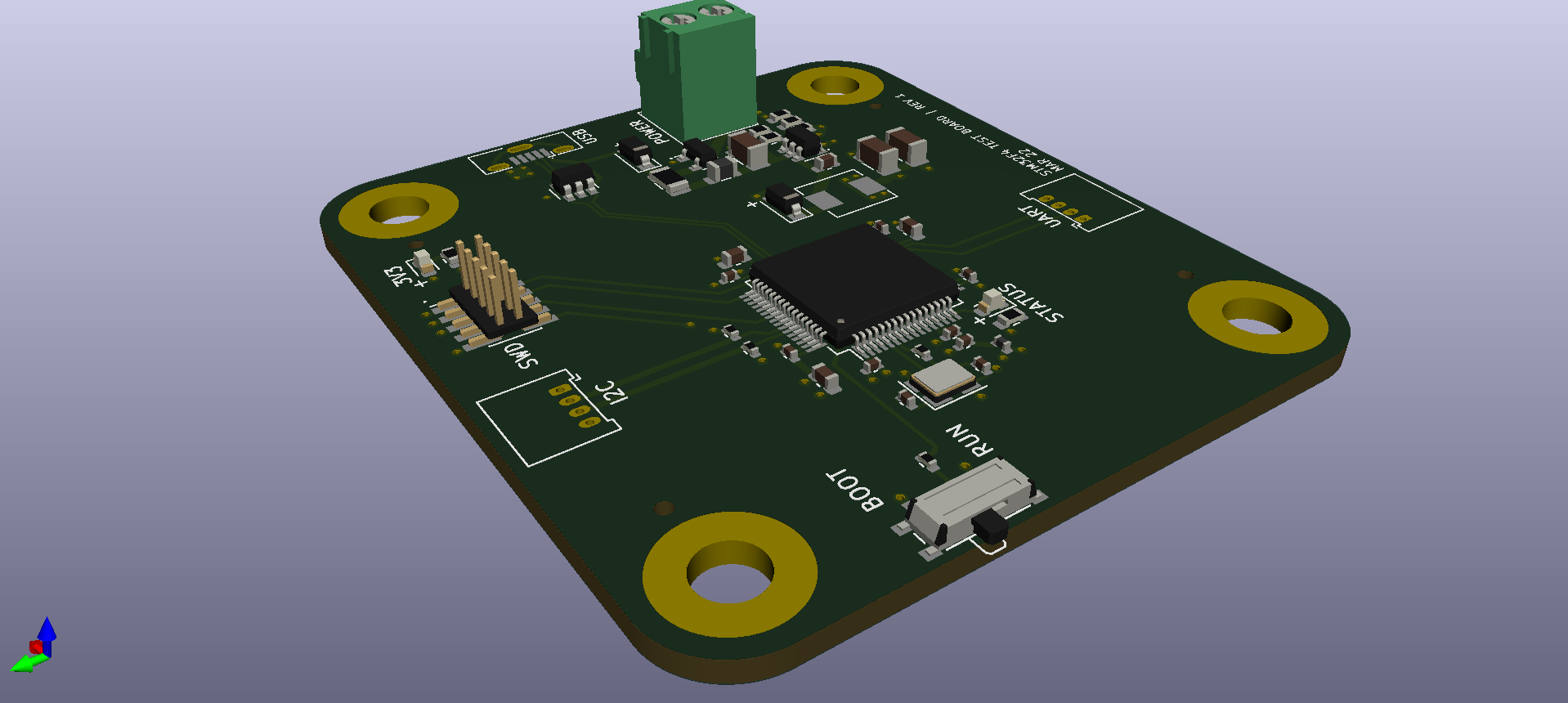
Rear angle — BOOT/RUN switches visible on left edge
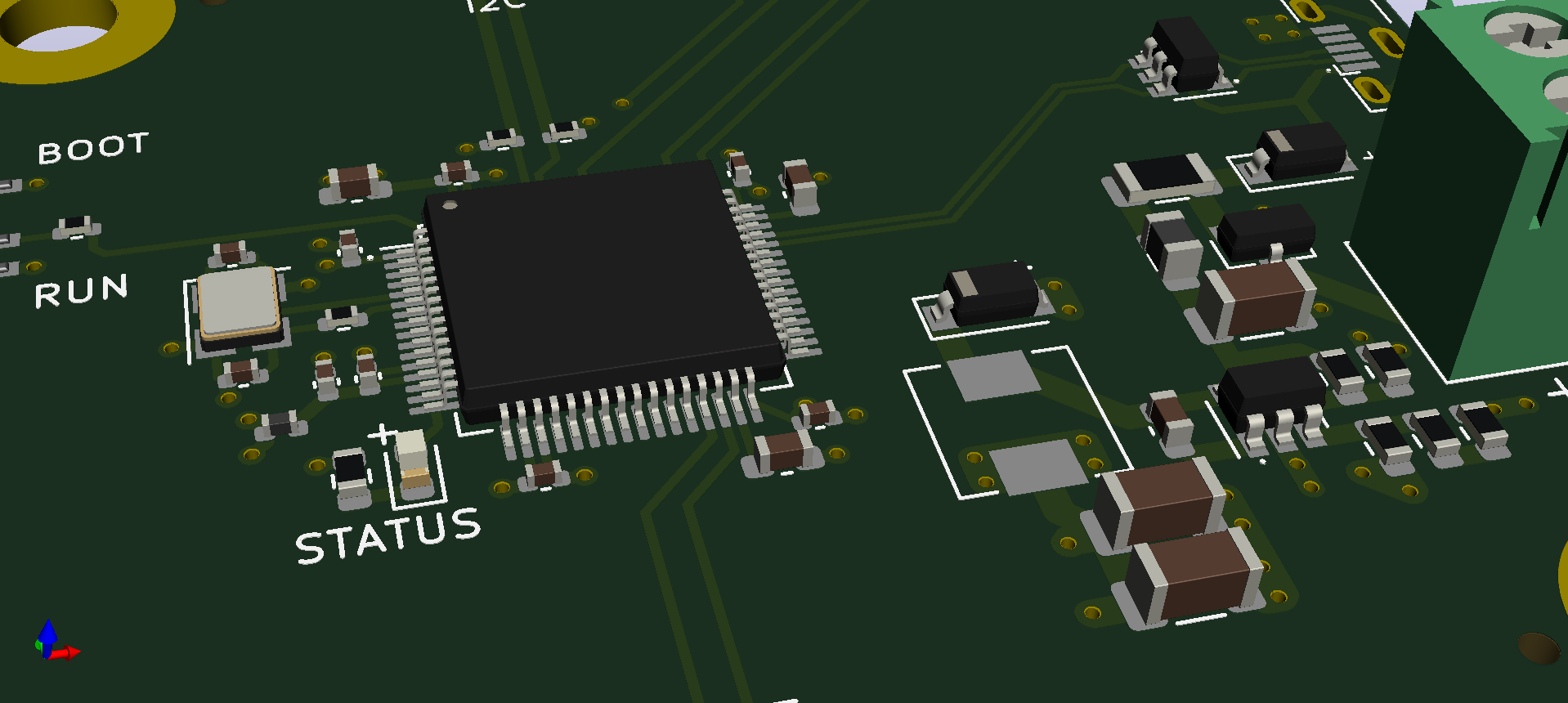
Close-up of STM32F405 centre-board, crystal lower-left, buck IC upper-right
Why This Board Exists
When learning embedded firmware development, most engineers use off-the-shelf Nucleo or Discovery boards. The problem is you don't control the hardware — you can't choose which peripherals are exposed, what power supply topology feeds the MCU, or how the debug interface is connected. Building your own development board forces you to understand every design decision from the datasheet level.
This board was designed to be a minimal but complete STM32 platform. It accepts 12V from a lab power supply or bench supply (via a 2-pin screw terminal), steps it down to 3.3V with a switching regulator, and exposes USB, SWD, I²C, and UART breakouts. The intention was to use this board as the compute core in future embedded projects that run from a 12V battery or power rail.
Every component on this board was researched from its datasheet before being placed in the schematic. The schematic includes hand-written annotations explaining design decisions (visible in the schematic PDF) — a practice that forces you to justify each choice rather than copying reference designs blindly.
Power Subsystem — Deep Dive
The power section is the most complex and most important part of this design. It converts 12V input to a clean, stable 3.3V rail that powers the STM32 and all peripherals.
Reverse Polarity Protection — Q1 (AO3401A P-Channel MOSFET)
The first component the 12V input hits is a P-channel MOSFET (Q1, AO3401A) acting as a reverse-polarity protection switch. This is a critical protection circuit: connecting a 12V supply backwards without protection would instantly destroy every chip on the board.
A Schottky diode could provide reverse polarity protection (it blocks current in reverse), but it has a forward voltage drop of ~0.3–0.5V. At 12V input and say 500mA load, that's 150–250mW of wasted power as heat — and the output voltage is no longer exactly 12V. A P-channel MOSFET in this configuration has an on-resistance of ~50–100mΩ, meaning the voltage drop at 500mA is only 25–50mV. It acts like a switch: almost zero drop when correct polarity, fully off (open circuit) with reverse polarity.
How it works: The P-channel MOSFET turns ON when V_GS is more negative than the threshold voltage (typically −1V to −2V). When 12V is applied correctly, the Source is at 12V and the Gate is pulled to GND (through D1), so V_GS = 0 − 12 = −12V → well below threshold → MOSFET is ON. With reversed polarity, the Source is near 0V and the Gate is pulled slightly above it, so V_GS ≈ 0 → MOSFET is OFF.
D1 (B5819W Schottky diode) protects the Gate of Q1 from being pulled more negative than −0.3V relative to the output (drain side), preventing oxide breakdown. The Schottky's low forward voltage (~0.3V) ensures the Gate is clamped precisely without wasting too much gate drive voltage.
Fuse F1 (250mA) and Ferrite Bead FB1 (600Ω @ 600 MHz)
After the MOSFET, there is a 250mA fuse (F1) in series. This is a sacrificial component: if something catastrophic occurs (a short on the board), the fuse blows open, disconnecting the input and protecting the power supply. The 250mA rating was chosen to cover the normal operating current of the board (~100–150mA at full load) with margin.
Following the fuse is a ferrite bead FB1 (600Ω @ 600 MHz). Ferrite beads behave as frequency-dependent resistors:
- At DC and low frequencies: nearly zero impedance (just wire) — does not affect power delivery
- At high frequencies (MHz range): high impedance — blocks high-frequency switching noise from propagating back toward the input connector and cable
A ferrite bead is a lossy inductor. Unlike a true inductor (which stores energy in its magnetic field and releases it), the ferrite material in the bead has high hysteresis losses at RF frequencies — it converts the high-frequency noise energy directly into heat rather than reflecting it back as a reactive impedance. This is why ferrite beads are used for EMI filtering rather than just inductors: they absorb noise energy rather than just blocking it. The 600Ω @ 600 MHz spec means at 600 MHz, the bead presents 600Ω of impedance, strongly attenuating any signals at that frequency.
Buck Converter — NP2399DJ-LF-Z (U1)
The heart of the power section is the NP2399DJ-LF-Z, a fixed-frequency PWM synchronous step-down (buck) converter. It converts the 12V input to a regulated 3.3V output.
A buck converter uses an inductor, capacitor, and high-frequency switching to step voltage down efficiently. Here is the principle step by step:
Phase 1 — Switch ON: The high-side switch closes, connecting the input (12V) to one end of the inductor L1. Current flows through the inductor and into the output capacitor and load. The inductor resists instantaneous current change (Faraday's law: V = L × dI/dt), so current ramps up linearly. Energy is stored in the inductor's magnetic field.
Phase 2 — Switch OFF: The high-side switch opens. The inductor, which cannot instantaneously stop current flow (its stored magnetic energy must go somewhere), forces current to continue flowing by pulling its input terminal negative. The catch diode D2 (B5819W Schottky) clamps this node to −0.3V, providing a return path for the inductor current through the load and back.
Output voltage regulation: By adjusting the duty cycle D (fraction of time the switch is ON), the average voltage at the switching node equals D × V_in. At steady state: V_out = D × V_in. For V_out = 3.3V and V_in = 12V: D = 3.3/12 = 0.275, so the switch is ON 27.5% of each switching cycle. The LC output filter (L1 + C2/C3) smooths the switching waveform into a stable DC.
Enable Circuit
The NP2399DJ's EN pin controls whether the converter runs. R1 (100kΩ) and R2 (68kΩ) form a voltage divider from BUCK_IN to GND, setting the EN pin voltage. This creates a UVLO (Undervoltage Lockout) function: the converter only enables when the input voltage is high enough that the divided voltage exceeds the EN threshold. This prevents the converter from trying to operate at very low input voltages where it might behave erratically.
Feedback Network — Output Voltage Setting
R3 (47kΩ), R4 (15kΩ), R5 (270Ω), and R12 (1kΩ) form the feedback resistor network that programs the output voltage. The converter's internal error amplifier compares the FB pin voltage to an internal 0.8V reference. The resistors divide the output voltage down to 0.8V when V_out equals the target.
Output Filter Components
| Component | Value | Function |
|---|---|---|
| L1 | 10 µH | Main buck inductor — stores/releases energy each switching cycle. Larger inductance = smaller ripple current but larger physical size and slower response. |
| D2 | B5819W Schottky | Catch/freewheeling diode — provides current path during switch-off phase. Schottky chosen for low forward voltage (~0.3V) to minimize conduction losses. |
| C2, C3 | 10 µF each (2 in parallel) | Output filter caps — smooth the switched voltage. Two in parallel reduce ESR (Equivalent Series Resistance) and provide more total capacitance for transient response. |
| C16 | 10 nF | Bootstrap capacitor — charges to V_out during the off-phase and boosts the gate drive voltage above V_in to fully enhance the high-side N-channel switch (if applicable to this IC topology). |
| C1 | 10 µF | Input bulk capacitor — absorbs the pulsed input current drawn during the switch-ON phase, preventing input voltage drooping. |
| D3 | RED LED + R3 | Power-good indicator — lights when 3.3V is present. Provides visual confirmation of power delivery during bring-up. |
Every capacitor has parasitic Equivalent Series Resistance (ESR) and Equivalent Series Inductance (ESL). At high switching frequencies, ESR causes the capacitor to appear resistive, and ESL causes it to appear inductive — both limit how well it can filter high-frequency ripple. Placing two capacitors in parallel halves the total ESR and ESL, improving the filter's effectiveness at the converter's switching frequency. This is a standard practice in switching power supply design.
Microcontroller Subsystem — STM32F405RGT6
The STM32F405RGT6 is a high-performance ARM Cortex-M4 MCU with FPU, running up to 168 MHz, with 1MB Flash and 192KB SRAM. It is significantly more capable than the typical STM32F103 used in many beginner development boards — chosen here because it supports USB OTG FS natively and has a hardware FPU for any signal processing applications.
16 MHz HSE Crystal Oscillator (Y1)
The STM32 has an internal RC oscillator (HSI at 16 MHz), but it has ±1% frequency accuracy — fine for most GPIO tasks, but not accurate enough for USB (which requires a timing source within ±0.25% of nominal). The external crystal Y1 (16 MHz) is orders of magnitude more accurate (~±20 ppm = 0.002%) and is required for USB operation.
Load Capacitor Calculation
The crystal datasheet specifies a load capacitance CL. The two external capacitors C14 and C15 (each 12 pF) provide this load in the Pierce oscillator configuration:
For a crystal specified at 8–12 pF load capacitance, 9 pF effective is correct. Using the wrong load caps shifts the crystal's resonant frequency — critical for USB timing accuracy.
R7 (47Ω) is a series resistor on the crystal output (OSC_OUT). It limits the drive current into the crystal, preventing overdrive — a phenomenon where too much drive current causes the crystal to oscillate in an overtone mode at a harmonic frequency, or damages the crystal over time through mechanical stress. The STM32 application note AN2867 recommends this resistor for most crystal configurations.
The STM32F405's PLL can multiply the HSE frequency up to 168 MHz (the CPU's maximum). With 16 MHz HSE, the PLL multiplier is set to ×21 and the AHB/APB dividers configured to produce common peripheral clock rates (48 MHz for USB, 84 MHz for APB2, 42 MHz for APB1). An 8 MHz crystal would work too but would require different PLL settings. 16 MHz is the value used in most ST reference designs.
VCAP Capacitors (C12, C13 — 2.2 µF each)
The STM32F405 has an internal 1.2V voltage regulator that powers the CPU core, caches, and internal logic. This regulator requires two external filter capacitors connected to the VCAP1 and VCAP2 pins to remain stable.
ST's datasheet is explicit: VCAP1 and VCAP2 must each have a 1µF to 4.7µF capacitor (low-ESR MLCC recommended). If these are omitted or have wrong values, the internal regulator oscillates and the MCU either fails to boot or runs erratically. Using 2.2µF (C12, C13) provides a comfortable margin within the specified range.
Decoupling Capacitors (C4–C9)
The STM32F405 in LQFP-64 has multiple VDD power pins (typically 4–6 pins for the core supply) and a separate VDDA pin for the analog domain (ADC, DAC, comparator). Each power pin needs its own decoupling capacitor placed as close to that pin as possible.
- C4 (4.7 µF): Bulk decoupling — provides charge reservoir for larger, slower current transients when the MCU switches between power states or executes memory-intensive code
- C5–C9 (100 nF each): High-frequency decoupling on individual VDD pins — absorbs the fast current spikes (nanosecond timescale) when digital logic switches states. Each 100nF cap services one VDD pin, placed in the immediate pin neighborhood.
Every time a logic gate switches (0→1 or 1→0), it demands a brief pulse of current from the power supply. This current must travel through the PCB traces and via inductance to the gate. Even a few nanohenries of trace inductance causes a voltage spike (V = L × dI/dt) on the supply rail that can corrupt neighbouring logic. A decoupling capacitor placed directly beside the chip acts as a local charge reservoir — it supplies that burst of current instantly from its own stored charge, without the spike having to travel back through the board. The speed at which a capacitor can supply charge depends on its ESR and ESL, which is why small-value ceramics (100nF 0402) work better at high frequencies than large electrolytics.
Analog Power Domain — 3.3VA (L2, C10, C11)
The VDDA pin (analog supply) is separated from the digital VDD by a ferrite bead L2 (39 nH) and filtered
with C10 (10 nF) and C11 (1 µF). This creates a distinct analog power domain (3.3VA) that is
isolated from the digital switching noise on the main 3.3V rail. Without this separation, the ADC would
measure noise from CPU instruction fetches, USB activity, and other digital events — degrading measurement
accuracy by adding a noise floor to every analog reading.
BOOT0 Switch and Reset
The STM32F405 determines its boot source on power-on by reading the BOOT0 pin:
| BOOT0 | Boot Source | Use Case |
|---|---|---|
LOW (0V) | User Flash (0x08000000) | Normal operation — runs the firmware stored in internal Flash |
HIGH (3.3V) | System Memory (bootloader) | DFU mode — connect USB and flash firmware without a programmer |
SW1 (BOOT slide switch) selects between these modes. R6 (10kΩ) pulls BOOT0 to GND by default (run firmware), and sliding the switch connects BOOT0 to 3.3V (enter bootloader). After toggling the switch, SW2 (RUN/NRST push button) resets the MCU, causing it to re-read BOOT0 and boot from the new source.
USB OTG FS — Full-Speed USB 2.0
The STM32F405 has a built-in USB OTG (On-The-Go) full-speed controller. OTG means the same port can act as either a USB host (connecting to a keyboard, flash drive, etc.) or a USB device (appearing as a CDC serial port, HID device, etc. to a PC). This is exposed via J5 (USB Micro B connector).
ESD Protection — USBLC6-2SC6 (U3)
USB connectors are one of the most frequently hot-plugged interfaces in any system. Every plug/unplug event can generate an electrostatic discharge (ESD) pulse of several kilovolts in microseconds — far exceeding the STM32's 1.5kV HBM (Human Body Model) ESD tolerance on GPIO pins.
The USBLC6-2SC6 is a bidirectional TVS (Transient Voltage Suppressor) array integrated into a 6-pin SOT-23 package. It contains two steering diodes per signal line (D+ and D−) that clamp transient voltages to safe levels before they can reach the STM32:
- Clamping voltage: typically 7–8V (well below the STM32's absolute maximum of 4V on GPIO)
- Response time: sub-picosecond — fast enough to catch even the fastest ESD events
- Parasitic capacitance: very low (~0.5 pF per line) — does not distort the USB signal waveform
The USBLC6-2SC6 must be placed as close to the USB connector as possible. ESD energy travels at near the speed of light on PCB traces — a device placed 10mm from the connector gives the ESD pulse 67ps to reach and damage the MCU before the suppressor can act. The suppressor's effectiveness drops dramatically with distance.
R9 and R10 (2.2kΩ each) are optional series resistors on D+ and D−. They damp reflections from impedance mismatches in the short trace between U3 and the STM32's USB pins.
Debug Interfaces
SWD — Serial Wire Debug (J2, 10-pin)
SWD (Serial Wire Debug) is ARM's 2-wire debug protocol, derived from JTAG but requiring only 2 signal lines instead of 4:
| SWD Pin | Function |
|---|---|
| SWDIO | Bidirectional data — carries debug commands, register reads/writes, memory access requests |
| SWCLK | Clock — driven by the debug probe, synchronises all transactions |
| SWO | Serial Wire Output (optional) — single-wire trace output. The STM32's ITM (Instrumentation Trace Macrocell) can output printf-style debug data here at high speed without stopping the CPU, unlike regular UART-based printf which blocks execution |
| NRST | Reset — the probe can assert a hardware reset, useful for stopping the CPU before it starts executing bad code during debug sessions |
JTAG requires 4+ pins (TCK, TDI, TDO, TMS, optional TRST). SWD achieves the same debugging capability with just 2 signals (SWDIO, SWCLK). On a board with few available pins, SWD is always preferred. The ARM Cortex-M4 core in the STM32F405 supports both protocols through the same physical pins — PA13/PA14 are JTMS-SWDIO and JTCK-SWCLK respectively, making them dual-function.
UART (J4) and I²C (J3) Breakout Headers
USART3 (TX on PC10, RX on PC11) is broken out to J4, a 4-pin header (TX, RX, +3.3V, GND). This allows a USB-UART converter (e.g., FTDI, CP2102) to be plugged in for printf debugging or command interface during development without occupying the USB OTG port.
I²C1 (SCL on PB10, SDA on PB11) is broken out to J3. I²C is a 2-wire bus (clock + data) that supports multiple devices on the same bus with different addresses. Common uses: OLED displays, IMU sensors (e.g., MPU-6050), temperature sensors, real-time clocks.
PCB Layout — 4-Layer Strategy
The board uses a 4-layer stackup. Here is why 4 layers rather than 2:
- Layer 1 (Top Signal): All component pads, primary signal routing
- Layer 2 (Ground Plane): Solid copper GND — provides return current path for all L1 signals, dramatically reduces loop inductance for decoupling capacitors, and acts as EMI shielding
- Layer 3 (Power Plane): 3.3V copper pour — distributes power from the buck converter output to all VDD pins without needing wide power traces on signal layers
- Layer 4 (Bottom Signal): Additional routing for connectors and power components
When a signal propagates along a PCB trace, its return current flows in the opposite direction through the nearest reference plane (ground). On a 2-layer board, there is no dedicated ground plane — return currents must find their own path through whatever ground copper is available, creating large current loops. Loop area is directly proportional to radiated EMI. A solid ground plane on L2 ensures that every signal on L1 has its return current flowing directly beneath it — minimal loop area, minimal EMI, and predictable 50Ω trace impedance for any future high-speed signals.
Component Placement Strategy
Looking at the board renders, the placement follows clear functional zones:
- Power zone (right side): Screw terminal J1 (12V in), Q1 MOSFET, F1 fuse, FB1 ferrite bead, U1 buck converter, L1 inductor, C1/C2/C3 capacitors. Power components are grouped together so high-current paths are short and don't cross under the MCU.
- MCU zone (centre): U2 STM32F405, decoupling caps immediately adjacent to each VDD pin, Y1 crystal as close to HSE_IN/OUT as possible.
- Interface zone (perimeter): J2 (SWD), J3 (I²C), J4 (UART) on the top edge; J5 (USB) on the right edge — all accessible without obstruction from the centre components.
- Control zone (left edge): SW1 (BOOT) and SW2 (RUN) switches on the left side, within easy reach for a finger during bring-up without needing to turn the board over.
Key Learnings
- Hands-on understanding of the complete KiCad workflow: schematic → PCB → Gerber → 3D render
- How to read IC datasheets and extract application circuit requirements, rather than copying reference designs
- Buck converter feedback network design from first principles — calculating resistor values from the target output voltage
- The importance of analog/digital power domain separation and how a ferrite bead implements it
- Crystal oscillator load capacitor calculation and the role of the series drive resistor
- USB ESD protection placement rules — the suppressor must be within 1mm of the connector
- 4-layer PCB stackup design and why a solid ground plane is non-negotiable for any design with USB or switching power