Mixed-Signal Hardware Design
— Signal Analyzer & Generator
A compact USB-powered mixed-signal instrument board featuring an STM32 microcontroller, precision ADC input, DAC output, and two BNC connectors for lab measurement integration. Designed to function as a low-frequency signal analyzer and waveform generator — a software-defined instrument built on custom hardware.
Board Renders
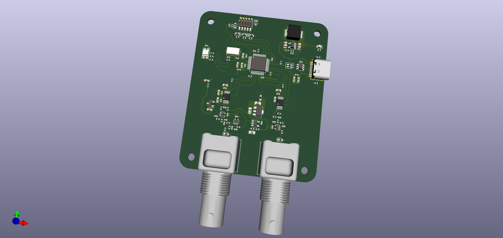
Top view — two BNC connectors dominate the left edge
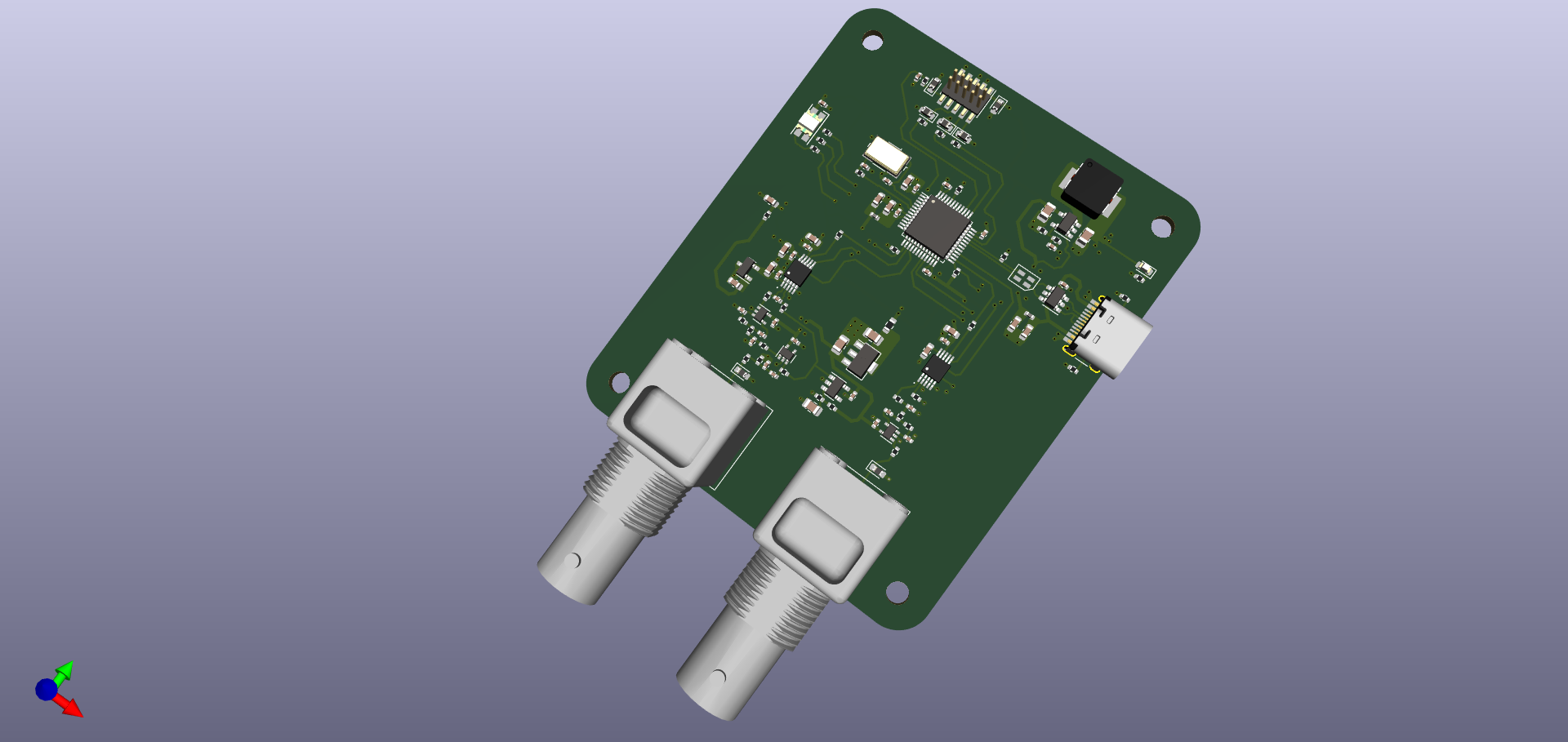
Angled view — compact form factor with USB Micro B top-right
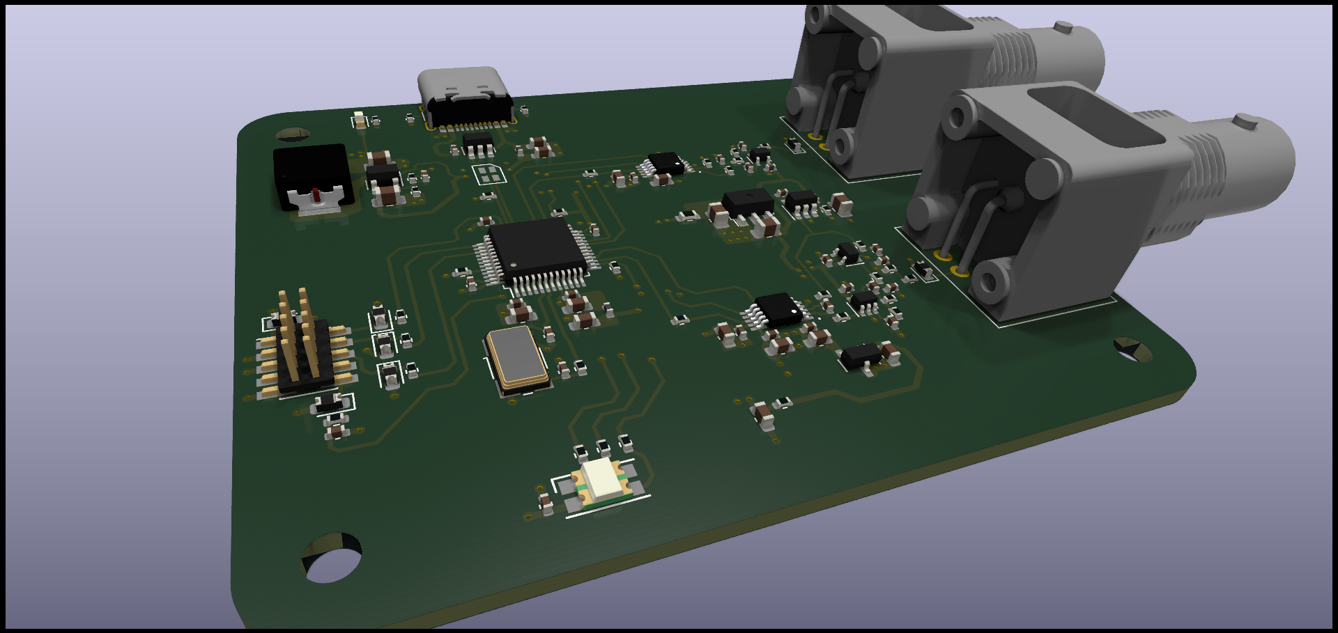
Render — bottom-left view showing BNC mechanical integration
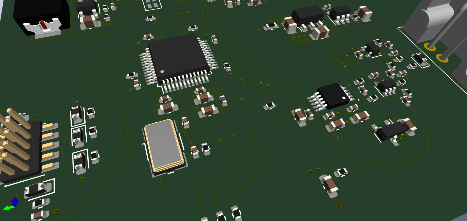
Close-up — STM32 centre, crystal oscillator visible below-left, signal chain components to the right
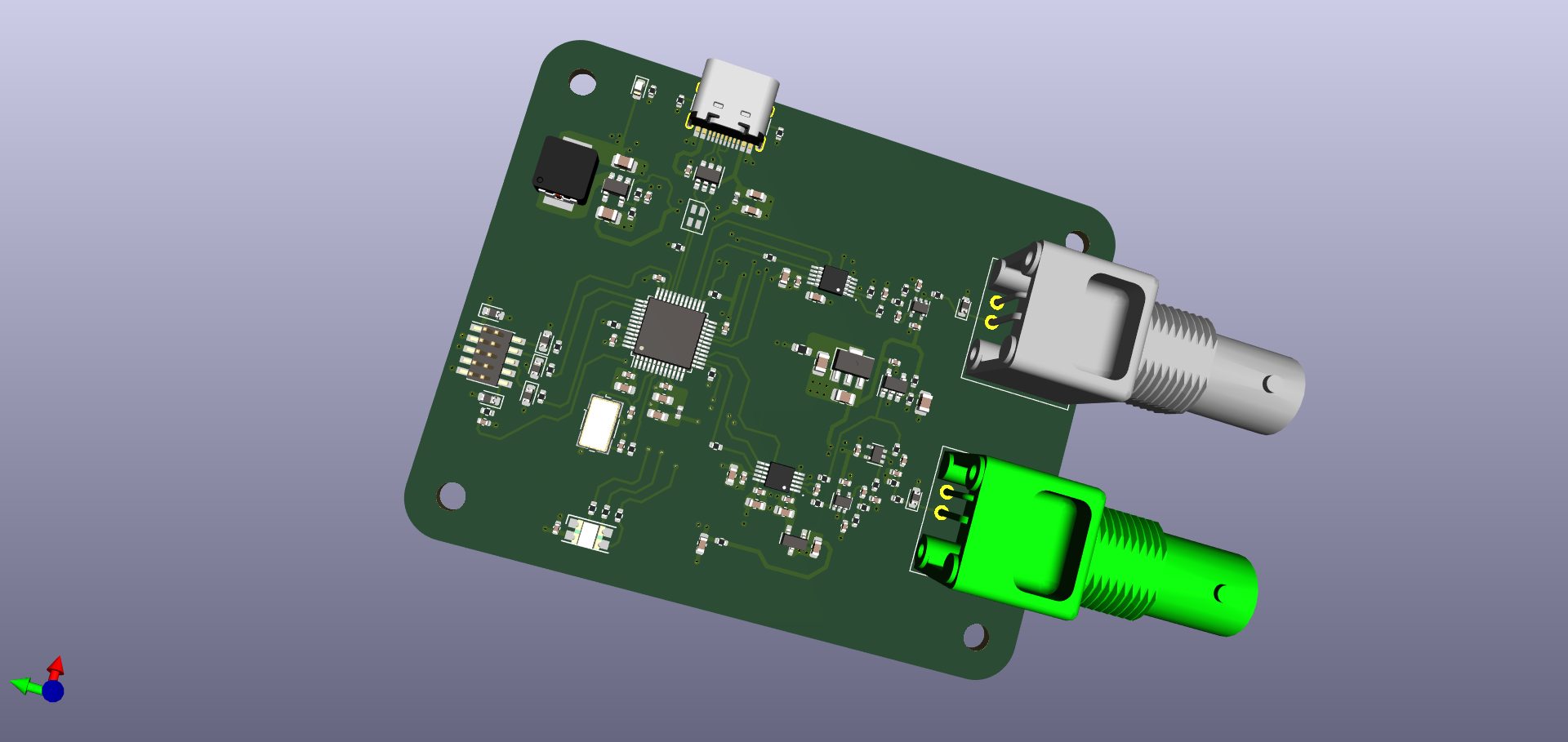
Alternate render — green screw terminal for secondary output/power access
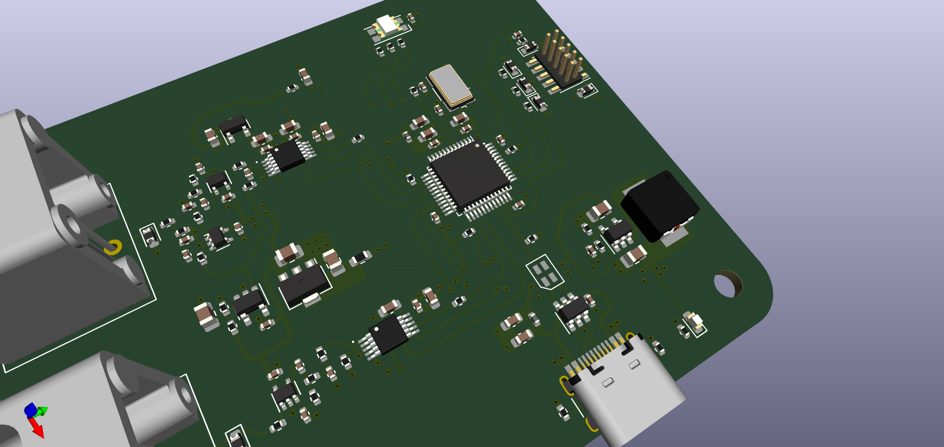
Component detail — mixed-signal routing visible around MCU
What This Board Does
This is a software-defined mixed-signal instrument. Rather than buying a separate function generator and oscilloscope, this board implements both in one compact PCB using the STM32's on-chip ADC and DAC:
USB CDC / HID
Generated signal
Measured signal
FFT, Analysis
The BNC connectors are the standard lab instrument interface — they allow this board to be connected directly to other instruments (oscilloscopes, signal generators, DUTs) using standard 50Ω coaxial cables, making it compatible with a professional lab environment.
One BNC is the input channel (ADC path — measuring an external signal). The other is the output channel (DAC path — generating a signal). Having both on the same board means the board can simultaneously generate a stimulus and measure the response — the fundamental workflow for impedance measurement, filter characterisation, and transfer function analysis.
Schematic Architecture — Four Sub-Sheets
The schematic is divided into four hierarchical sub-sheets in KiCad, each responsible for one functional block. This is a good practice for complex designs — it keeps each sheet focused and manageable, and allows the top-level sheet to show the overall system architecture without drowning in component details.
Power.kicad_sch — USB Power Regulation
The board is powered entirely via the USB Micro B connector (J1). USB 2.0 provides 5V at up to 500mA on VBUS. The power sub-sheet steps this down to 3.3V for the MCU and signal chain.
A simple 3-terminal linear regulator (e.g., AMS1117-3.3) could drop 5V to 3.3V, but it wastes the difference as heat: P_waste = (V_in − V_out) × I_load = 1.7V × 200mA = 340mW. That's a significant temperature rise on a small board. For mixed-signal applications this is especially problematic: heat changes component values (resistors, capacitor dielectric, crystal frequency) and introduces thermal noise.
The preferred solution at low currents is a low-dropout (LDO) regulator with low quiescent current, placed away from the analog signal path. A small ferrite bead between the digital and analog power domains ensures switching noise from the MCU doesn't contaminate the ADC reference.
The analog supply (AVDD) is filtered separately from the digital VDD through a ferrite bead and extra bypass capacitors. This is the same technique used in the STM32 test board — it is essential in any design where the ADC needs to achieve better than 8-bit accuracy.
ADC.kicad_sch — Signal Input & Conditioning
The ADC sub-sheet handles everything between the BNC input connector and the STM32's ADC pin. Raw signals arriving at a BNC connector cannot be fed directly into a microcontroller ADC — they need conditioning first.
Signal Conditioning Chain
| Stage | Component Type | Why It's Needed |
|---|---|---|
| 1. Input protection | Clamping diodes / TVS | Prevents voltages above 3.3V or below 0V from reaching the ADC pin, which can permanently damage the MCU. The STM32's ADC input is only rated 0 to VDDA (3.3V). |
| 2. Anti-aliasing filter | RC low-pass filter | The Nyquist theorem requires that all signal components above half the sampling rate be removed before sampling, or they "alias" into the passband as false lower-frequency signals. For a 100 kSa/s ADC, any signal component above 50 kHz must be filtered out. |
| 3. DC bias / offset | Resistor divider or op-amp | The STM32 ADC measures 0 to 3.3V. An AC signal centred at 0V (which swings from −1V to +1V) cannot be measured directly — its negative portion would be clamped. A bias network shifts the signal up so 0V AC maps to 1.65V (VDDA/2) at the ADC input. |
When you sample a continuous signal at a rate f_s, you can only accurately reconstruct frequencies up to f_s/2 (the Nyquist frequency). Any frequency component above f_s/2 in the input signal "folds back" into the 0 to f_s/2 range — it appears as a false, lower-frequency signal indistinguishable from a real one. This is called aliasing. The anti-aliasing filter's cutoff frequency must be ≤ f_s/2 to prevent this. For example, with 100 kSa/s ADC sampling, an anti-aliasing filter at 40 kHz ensures all frequencies above 40 kHz are attenuated before they can be sampled and create alias artefacts.
DAC.kicad_sch — Signal Generation & Output
The DAC sub-sheet handles signal generation — converting the STM32's digital waveform data into an analog voltage, then driving it through the BNC output connector.
The Challenge: MCU DAC Output Impedance
The STM32's internal DAC has an output impedance of several kilohms. Connected directly to a 50Ω BNC cable and load, the signal would be severely attenuated (voltage divider: V_out = V_dac × 50 / (50 + R_out) — essentially nothing would come out). A buffer amplifier is needed between the DAC output and the BNC connector.
Any signal source has an internal (Thevenin) output impedance. When a load is connected, voltage divides between this source impedance and the load: V_load = V_source × R_load / (R_load + R_source). A 50Ω coaxial cable terminated at 50Ω presents a 50Ω load to the source. If the source (DAC) has 3kΩ output impedance, the signal level at the cable end is V × 50/(50+3000) = V × 0.016 — only 1.6% of the generated voltage actually reaches the destination. A voltage buffer (unity-gain op-amp follower) with near-zero output impedance solves this: the op-amp's feedback forces its output to equal its input regardless of load current, so a 50Ω load draws current from the op-amp's output stage rather than from the high-impedance DAC.
Output Filtering
The DAC output is a stepped waveform — each sample is held at its value until the next sample (zero-order hold). This creates images of the signal at multiples of the sample rate. A reconstruction filter (low-pass at or below f_s/2) smooths these steps into a clean analog waveform. Without it, the "generated sine wave" would look like a staircase at low zoom, contaminating measurements with high-frequency harmonics.
MCU.kicad_sch — STM32 Core and USB Interface
The MCU sub-sheet contains the STM32 microcontroller, its support components (crystal, decoupling, reset), and the USB interface that connects to the host PC.
The STM32's internal DMA (Direct Memory Access) controller is essential here: it allows the ADC to continuously fill a memory buffer and the DAC to continuously drain a memory buffer without CPU involvement. The CPU can be simultaneously processing FFTs on previously captured data, running USB communication, and updating a display — while the DMA independently manages the real-time ADC/DAC streams at a precise, timer-controlled sample rate.
The board enumerates as a USB CDC (Communications Device Class) device — it appears as a virtual COM port to the PC. Captured waveform data is streamed from the MCU to the PC over this virtual serial link at USB Full Speed (12 Mbps). A Python or MATLAB script on the PC reads this stream, reconstructs the time-domain waveform, and optionally performs FFT for frequency-domain analysis.
Mixed-Signal PCB Design Principles Applied
A "mixed-signal" PCB is one that contains both digital circuits (MCU, USB, oscillators) and analog circuits (ADC input path, DAC output path, op-amp buffers, BNC connectors) on the same board. The fundamental challenge is preventing the noisy digital circuits from contaminating the sensitive analog circuits.
Ground Plane Partitioning — The Most Critical Decision
The ground plane is the single most important factor in mixed-signal PCB performance. There are two schools of thought:
- Separate analog and digital ground planes — joined at a single point (star ground). Prevents digital return currents from flowing through the analog ground. Risk: the star point must be carefully chosen, and the seam between planes can create impedance discontinuities.
- Single solid ground plane — used throughout. Digital and analog circuits all share the same plane. Component placement is used to keep analog components physically away from digital ones, so return currents naturally stay in their own regions. This is the approach recommended by Henry Ott and most modern signal integrity experts.
The single-plane approach works because return currents flow in the path of least impedance — which at high frequencies is directly beneath their forward-current trace. If analog and digital traces are kept separated on the board, their return currents will also stay separated in the underlying plane — achieving the same isolation effect without the risk of a poorly placed star point.
BNC Connector — 50Ω Impedance Standard
BNC (Bayonet Neill–Concelman) connectors are the universal standard for lab instrument signal connections. They use coaxial geometry — a centre signal conductor surrounded by a coaxial outer shield (ground) — with a characteristic impedance of 50Ω.
Any conductor carrying a signal has distributed inductance and capacitance per unit length. At high enough frequencies (or long enough cables), the signal propagates as a wave rather than an instantaneous change. When this wave hits an impedance discontinuity (e.g., a 50Ω cable connecting to a 1MΩ oscilloscope input), a reflection occurs — part of the energy bounces back toward the source. These reflections create signal integrity problems (ringing, overshoot, incorrect amplitude readings). Terminating the cable with a resistor equal to the cable's characteristic impedance (50Ω) eliminates reflections entirely. The 50Ω standard was chosen as a compromise between power handling (which favours higher impedance) and signal bandwidth (which favours lower impedance at RF frequencies).
Key Learnings
- Mixed-signal PCB partitioning — understanding where digital noise enters the analog signal path and how ground plane strategy controls it
- Anti-aliasing filter design: calculating RC values based on sample rate, understanding the Nyquist theorem and aliasing artefacts
- DAC output buffering: why output impedance matters and how an op-amp follower solves the loading problem
- BNC connector selection and the significance of 50Ω impedance matching in lab instrument design
- Hierarchical schematic design in KiCad — splitting a complex design into functional sub-sheets for clarity and maintainability
- USB CDC implementation on STM32 — enumerating as a virtual COM port and streaming data to a host PC
- DMA-based ADC/DAC operation: achieving precise, CPU-independent sample timing for accurate frequency measurements