Power Filter Test Board
— C, LC, and Pi Filter Comparison
A characterisation board designed to compare three power supply filter topologies side by side — a simple capacitor filter, an LC filter, and a Pi (π) filter — on the same PCB, with switchable inputs and a BNC output for direct oscilloscope or VNA measurement. Built in Altium Designer as a hands-on tool for understanding power integrity on PCBs.
System Architecture
The board's architecture was carefully thought out to make filter comparison as clean as possible. Every filter sees the same source impedance and the same load — only the filter topology changes.
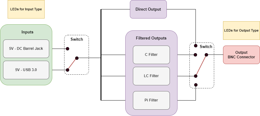
Architecture diagram — drawn in draw.io showing the complete signal/power flow
The diagram reveals the elegant two-switch architecture:
- Input switch: Selects between 5V DC barrel jack and 5V USB 3.0 — both provide the same nominal voltage but with different source impedances and noise characteristics. This allows the filters to be characterised under different upstream conditions.
- Direct path: Bypasses all filters entirely — the raw input goes straight to the output switch. This provides the unfiltered reference measurement showing exactly how much noise is present before any filtering.
- Three filtered paths: C filter, LC filter, and Pi filter — each running in parallel from the same input. The output switch selects which filtered (or direct) output goes to the BNC.
- Status LEDs: Separate LEDs indicate which input is active and which output topology is selected — preventing measurement errors from ambiguity about board state.
- BNC output: Single coaxial output for clean connection to an oscilloscope or VNA (Vector Network Analyser).
Without a reference measurement (no filter), you cannot know how much attenuation each filter provides. The direct path reveals the noise floor, ripple amplitude, and spectral content of the input source itself. Every filter measurement is then compared against this baseline. This is standard practice in power integrity characterisation — always measure before and after to quantify improvement.
The Three Filter Topologies — Complete Physics Walkthrough
Each filter topology is a different arrangement of inductors and capacitors. Understanding why each one behaves differently requires understanding what inductors and capacitors actually do to AC signals.
A capacitor's impedance (how much it resists current flow) decreases with increasing frequency: Z_C = 1/(2πfC). At DC (f=0), a capacitor is an open circuit. At high frequency, it's nearly a short circuit. This makes capacitors excellent at shunting high-frequency noise to ground.
An inductor's impedance increases with frequency: Z_L = 2πfL. At DC, an inductor is nearly a short circuit (just wire resistance). At high frequency, it's a high impedance. This makes inductors excellent at blocking high-frequency noise from passing through.
Low-pass filters exploit these properties: inductors block high-frequency noise in series, capacitors shunt high-frequency noise to ground in parallel.
IN ──┬── OUT
     │
    [C]
     │
    GND
A single capacitor from the power rail to ground. The simplest possible filter.
IN ──[L]──┬── OUT
          │
         [C]
          │
         GND
Series inductor + shunt capacitor. Steeper rolloff and better high-frequency rejection than C alone.
IN ─┬─[L]─┬─ OUT
    │      │
   [C1]  [C2]
    │      │
   GND   GND
Two shunt capacitors with a series inductor between them. Highest attenuation of the three.
Stage 1: The Capacitor Filter
The single-capacitor filter is the most basic noise reduction technique. Connecting a capacitor from the power rail to ground creates a shunt path for high-frequency noise:
- At DC: the capacitor is an open circuit — no current flows, full DC voltage reaches the load
- At 1 MHz: Z_C = 1/(2π × 1MHz × 10µF) = 0.016Ω — the capacitor is nearly a short circuit to ground, diverting the 1 MHz noise away from the load
In a real circuit, the capacitor works against the source impedance R (the wiring resistance, trace resistance, and source output impedance). Together they form an RC low-pass filter with cutoff frequency f_c = 1/(2πRC). Below f_c, signals pass through with little attenuation. Above f_c, each decade of frequency increase causes 20 dB (10×) of additional attenuation.
The critical limitation of a single capacitor filter: if the source impedance R is very low (as with a lab power supply or USB port), f_c is pushed to very high frequencies and the filter barely attenuates anything at audio/power supply frequencies. The only way to improve it without adding an inductor is to use a larger capacitor value.
ESR — the capacitor's fatal flaw at high frequency: Every physical capacitor has parasitic series resistance (ESR) and inductance (ESL). At some frequency (the self-resonant frequency, SRF), the capacitor's impedance stops decreasing and starts increasing — it now looks like an inductor. Above the SRF, the C filter stops working. The board allows this phenomenon to be directly observed by measuring filter attenuation from low frequency to hundreds of MHz.
Stage 2: The LC Filter
Adding a series inductor before the shunt capacitor creates an LC filter with dramatically better performance. Now both components work together:
- The inductor presents high impedance to high-frequency noise, blocking it from passing to the load at all
- The capacitor provides a low-impedance shunt path to ground, diverting whatever noise gets past the inductor
These two mechanisms compound: at 10× above the cutoff frequency, the inductor's impedance is 10× higher AND the capacitor's impedance is 10× lower, giving 100× (40 dB) total attenuation per decade — versus 10× (20 dB) for a C filter alone.
The LC filter has a resonant frequency f_0 = 1/(2π√LC) where the inductor and capacitor exchange energy at a natural rate. At resonance, the impedance of the series combination drops to nearly zero (limited only by parasitic resistance). This creates a peak in the transfer function at f_0 — signals at the resonant frequency are actually amplified, not attenuated!
This resonant peak is visible when measuring the LC filter with a VNA or by injecting a swept-frequency signal and measuring the output. Above resonance, attenuation is −40 dB/decade. The quality factor Q of the resonance determines how sharp the peak is — a high-Q (low damping) filter has a sharp resonant peak and fast rolloff; a low-Q (high damping) filter has a more gradual transition but no peaking. Adding a damping resistor in series with the inductor reduces Q and smooths the response.
LC Filter Design Equation
Stage 3: The Pi (π) Filter
The Pi filter adds a second shunt capacitor at the input side of the inductor, creating a three-component topology that looks like the Greek letter π (pi): capacitor–inductor–capacitor. This is the highest-performing of the three topologies, achieving −60 dB/decade rolloff.
The Pi filter's operating principle combines all three effects:
- C1 (input capacitor): First noise reduction stage — shunts high-frequency noise directly at the input, before it even reaches the inductor. This reduces the noise amplitude the inductor must deal with.
- L (series inductor): Second stage — blocks the remaining noise from passing to the output side.
- C2 (output capacitor): Third stage — shunts any residual noise that leaked through the inductor to ground at the output.
There is also a T-filter (inductor–capacitor–inductor). Pi and T filters have the same order (3rd order) and the same theoretical rolloff (−60 dB/decade). The difference is their terminal impedances:
• Pi filter: shunt elements at both ends → low input and output impedance. Works best when source and load impedances are HIGH.
• T filter: series elements at both ends → high input and output impedance. Works best when source and load impedances are LOW.
For power supply filtering where the source (5V supply) has low impedance and the load is typically capacitive (IC decoupling caps), the Pi filter is the correct choice — its shunt input capacitor absorbs noise from the low-impedance source, and the shunt output capacitor charges the IC's bypass capacitors.
The Pi Filter's Advantage: Input Noise Pre-Absorption
The first capacitor C1 has a subtle but important benefit: it pre-absorbs noise on the input rail before that noise induces current through the series inductor. In an LC filter, the inductor must carry the full noise current as the capacitor charges. In a Pi filter, C1 handles the initial noise spike, and the inductor only sees the residual — a much smaller current. This reduces the voltage drop across the inductor's DC resistance and improves the dynamic response to load steps.
Using the Board for Characterisation
The board's BNC output connects to an oscilloscope or vector network analyser. With a signal generator injecting noise into the input, the filter transfer functions can be plotted directly:
| Measurement | Instrument | What It Shows |
|---|---|---|
| Time domain noise floor | Oscilloscope (AC coupling) | Peak-to-peak ripple voltage on each filter output vs direct output |
| Frequency response (Bode plot) | VNA or spectrum analyser + signal gen | Attenuation vs frequency — shows cutoff frequency, rolloff slope, and resonant peak of LC/Pi filters |
| Step response | Oscilloscope + load step circuit | How quickly each filter allows the output voltage to recover after a sudden current demand — measures transient response |
| Source comparison | Oscilloscope, switching vs USB input | Whether the DC barrel jack (from a switching adapter) or USB 3.0 has more noise — reveals the filter's effectiveness under different real-world conditions |
LTSpice can simulate ideal filters perfectly. But the real board exposes effects that simulation misses: capacitor self-resonance, inductor core saturation at high current, PCB trace inductance adding to the filter's inductance, and ground plane coupling. Measuring a physical board with real instruments is the only way to verify that simulation predictions hold in practice — and to discover the parasitic effects that need to be modelled more carefully.
Altium Designer Implementation
This board was designed in Altium Designer, a professional EDA tool used in commercial electronics development. Moving from KiCad (used in the STM32 board) to Altium for this project required learning a new tool chain while applying the same fundamental design principles.
Key Altium Features Used
- Hierarchical design: The main schematic and power filter sub-sheets were linked via ports, keeping the topology clean
- Net classes: Power nets (5V, GND) were assigned thicker trace widths in the PCB rules — power traces need lower resistance for lower I²R losses
- Design Rule Check (DRC): Automated checking verified clearances between high-voltage components, trace widths, and drill sizes before generating Gerbers
- Interactive routing: Altium's differential pair router and length-matching tools, though not strictly needed for this low-speed design, were practised for future high-speed projects
- 3D body models: All components had assigned 3D body models (STEP files) enabling realistic 3D renders and mechanical interference checking
- Engineering Change Orders (ECO): 25 ECO log files track every design revision — a professional workflow for documenting changes
Component Selection for Filters
Component selection for the filter elements involved balancing several trade-offs:
| Component | Key Parameter | Selection Rationale |
|---|---|---|
| Filter Inductors | Core material, DCR, SRF | Ferrite core inductors chosen for their high permeability and good high-frequency performance. DCR (DC resistance) must be low to avoid voltage drop. SRF must be above the frequency range of interest. |
| Input/Output Caps (C filter) | ESR, capacitance value, voltage rating | X5R/X7R MLCC chosen for low ESR. Voltage rating derated 2× (25V cap for 5V rail) for reliability and to keep capacitance near rated value (MLCCs lose capacitance under DC bias). |
| Pi Filter Caps (C1, C2) | Self-resonant frequency matching | C1 and C2 can be different values — C1 (larger) provides low-frequency filtering, C2 (smaller) handles high-frequency residuals. The combination extends the effective filtering bandwidth beyond what either cap could achieve alone. |
| Input switch | Current rating, contact resistance | Rated well above the maximum expected current. Low contact resistance ensures the switch doesn't add significant source impedance that would change the filter's response. |
Key Learnings
- Deep understanding of C, LC, and Pi filter topologies — not just equations but the physical mechanisms (energy storage, reactance, impedance matching) that make each one work
- Capacitor ESR and self-resonance — why a capacitor's filtering effectiveness is frequency-limited and how to choose the right type for the target frequency range
- The LC resonant peak — how to predict its frequency, measure it with a VNA, and add damping if it causes instability
- Pi vs T filter topology selection based on source and load impedance
- The importance of a direct (unfiltered) reference path in any characterisation board
- Transitioning from KiCad to Altium Designer — professional EDA workflow, ECO logs, and design rules
- How switching power supply ripple and USB power noise differ spectrally, and which filter topology handles each better