Op-Amp Characterization in LTspice
A full SPICE characterization of an operational amplifier against its datasheet — DC offsets and bias currents, differential and common-mode gain, CMRR and PSRR, unity-gain bandwidth, and step-response slew rate — with every parameter measured, plotted, and compared to spec.
The goal: treat a datasheet as a spec to verify
A datasheet makes a lot of promises — an offset voltage here, a CMRR there, a unity-gain bandwidth on the last page. The point of this project was to take those promises and verify every one of them in simulation, the same way you'd characterize a real part on the bench: build the right test setup for each parameter, measure it, and put the result next to the specified value.
It's a compact version of exactly the mixed-signal characterization mindset I use professionally — decide what "good" means, build a repeatable measurement for it, and let the numbers, not intuition, tell you whether the part meets spec.
Results at a glance
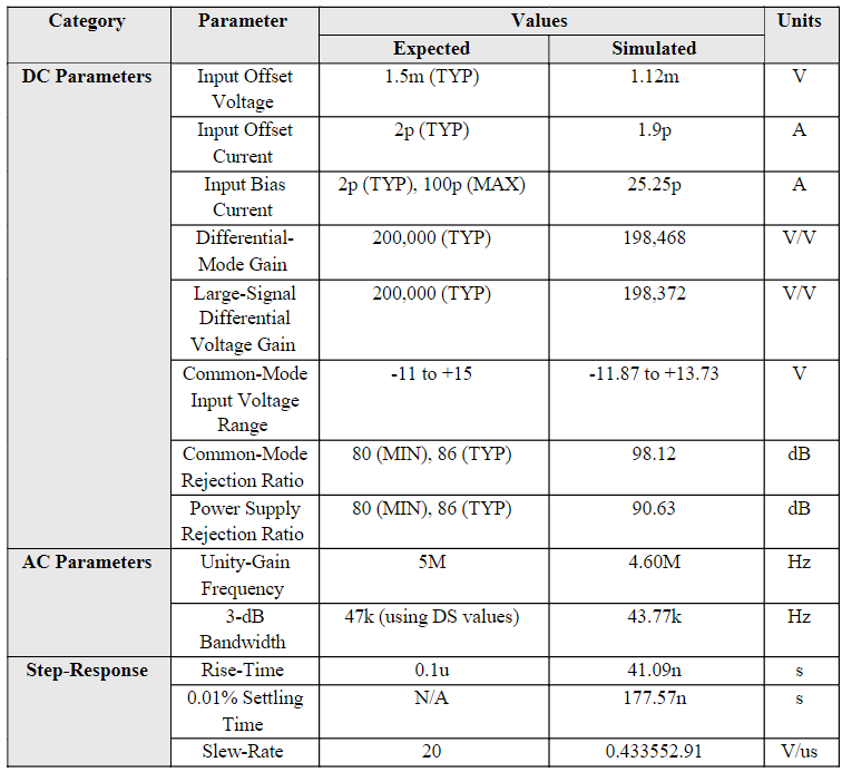
Every parameter, expected vs. simulated, in one table. This is the deliverable the whole project builds toward — a single sheet you could hand to someone and say "here's how this part actually behaves."
DC parameters — offsets, bias, and rejection
The DC tests pin down the amplifier's static, real-world imperfections — the things an ideal op-amp wouldn't have:
| Parameter | What it measures | My result |
|---|---|---|
| Input offset voltage | The small differential voltage needed to drive the output to zero — mismatch in the input stage. | ≈ 1.12 mV |
| Input bias / offset current | The tiny current the inputs actually draw, and the mismatch between them. | ≈ 25 pA / 1.9 pA |
| Differential-mode gain (Avd) | Open-loop gain on a differential input — how hard the amp amplifies the signal you want. | ≈ 198,000 V/V |
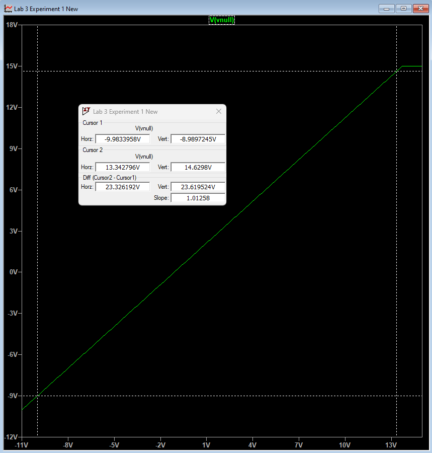
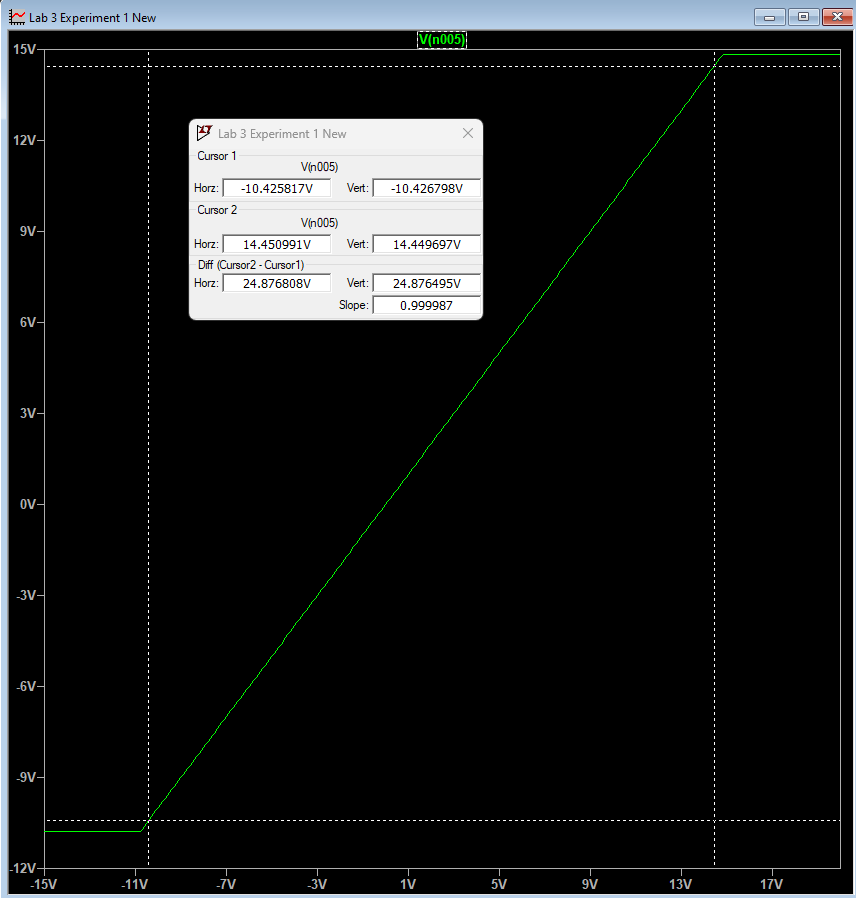
| CMRR | How well it rejects a signal common to both inputs vs. amplifying the difference. | ≈ 98 dB |
| PSRR | How well it rejects noise/ripple riding on its supply rails. | ≈ 91 dB |


AC parameters — gain across frequency
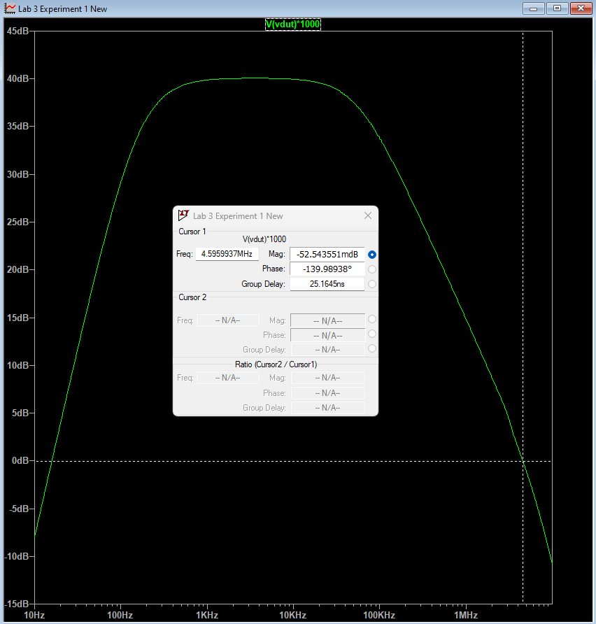
An AC sweep turns the amplifier's single open-loop gain number into a curve, and two points on that curve matter most: the 3-dB bandwidth (≈ 43.8 kHz here, where gain has fallen 3 dB) and the unity-gain frequency (≈ 4.6 MHz, where the gain finally crosses 0 dB). Their product is roughly constant — the classic gain-bandwidth trade — so knowing one tells you what closed-loop bandwidth you can buy at a given gain.
Step response — slew rate and settling
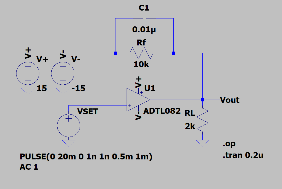
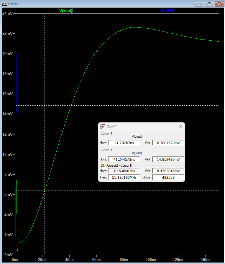
The transient tests push a step into the amplifier and watch how fast it can actually move. Slew rate is the maximum output rate of change (V/µs) — a large-signal limit that a small-signal bandwidth number won't warn you about — and settling time is how long the output takes to land within a tolerance band of its final value (≈ 178 ns to 0.01% here). Rise time came out at ≈ 41 ns.
What I took away from it
- Building a separate, correct test setup per parameter — DC operating-point sweeps for offsets and rejection, AC for gain/bandwidth, transient for slew and settling.
- Reading an amplifier the way a validation engineer does: CMRR, PSRR, offset, gain-bandwidth and slew as the handful of numbers that decide whether it works in a real signal chain.
- Comparing measured behaviour against a datasheet spec and being able to explain the deltas (e.g. simulated ≈ 98 dB CMRR vs. an 86 dB typical).
- The same discipline — define the metric, build the measurement, compare to spec — that post-silicon characterization runs on, just at the board/SPICE level.