Signal Analyzer & Generator
A compact USB-powered mixed-signal instrument: an STM32 with a precision ADC input, a DAC output, and two BNC connectors. A software-defined low-frequency signal analyzer and waveform generator built on custom hardware.
Board renders
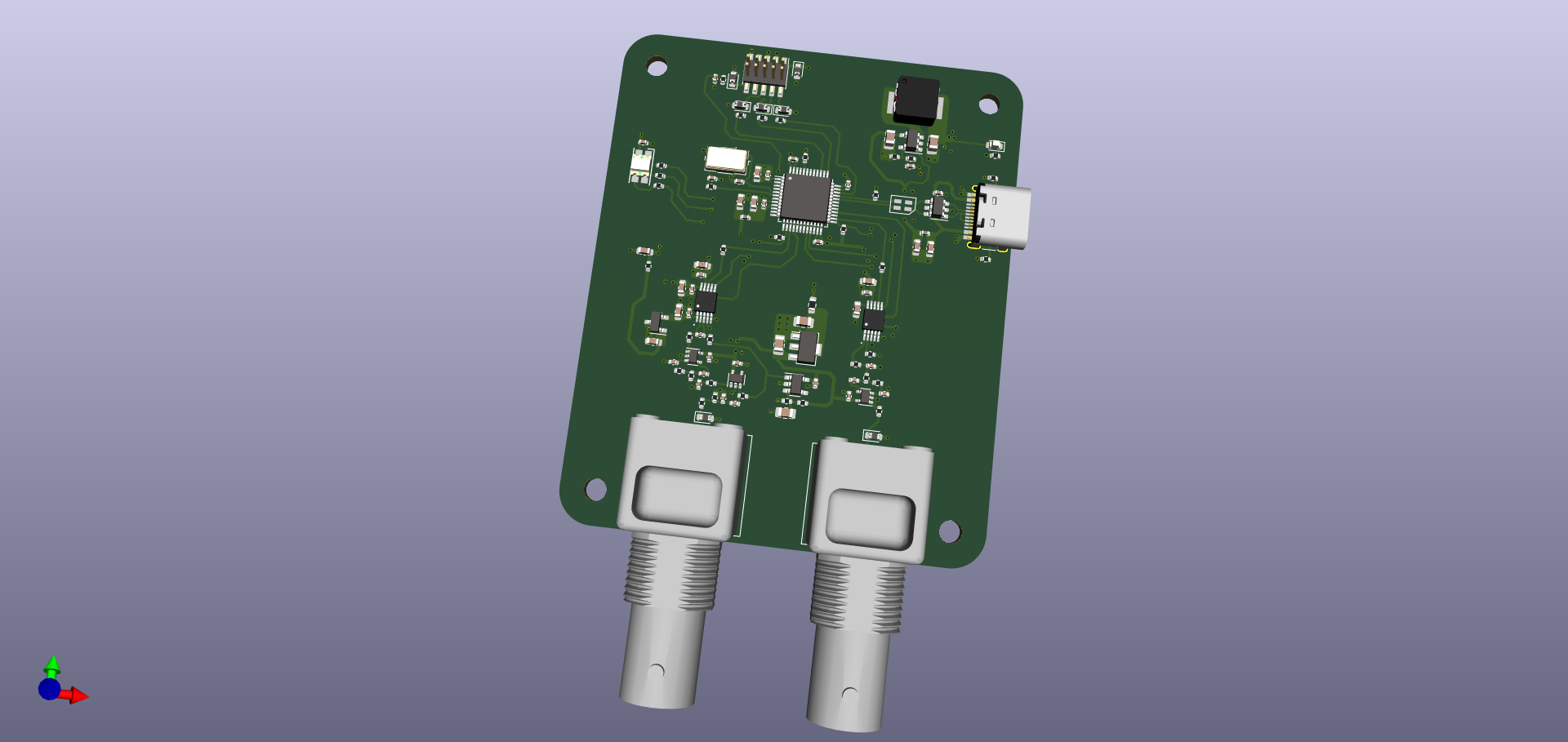
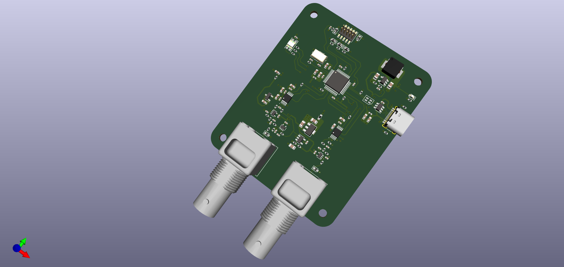
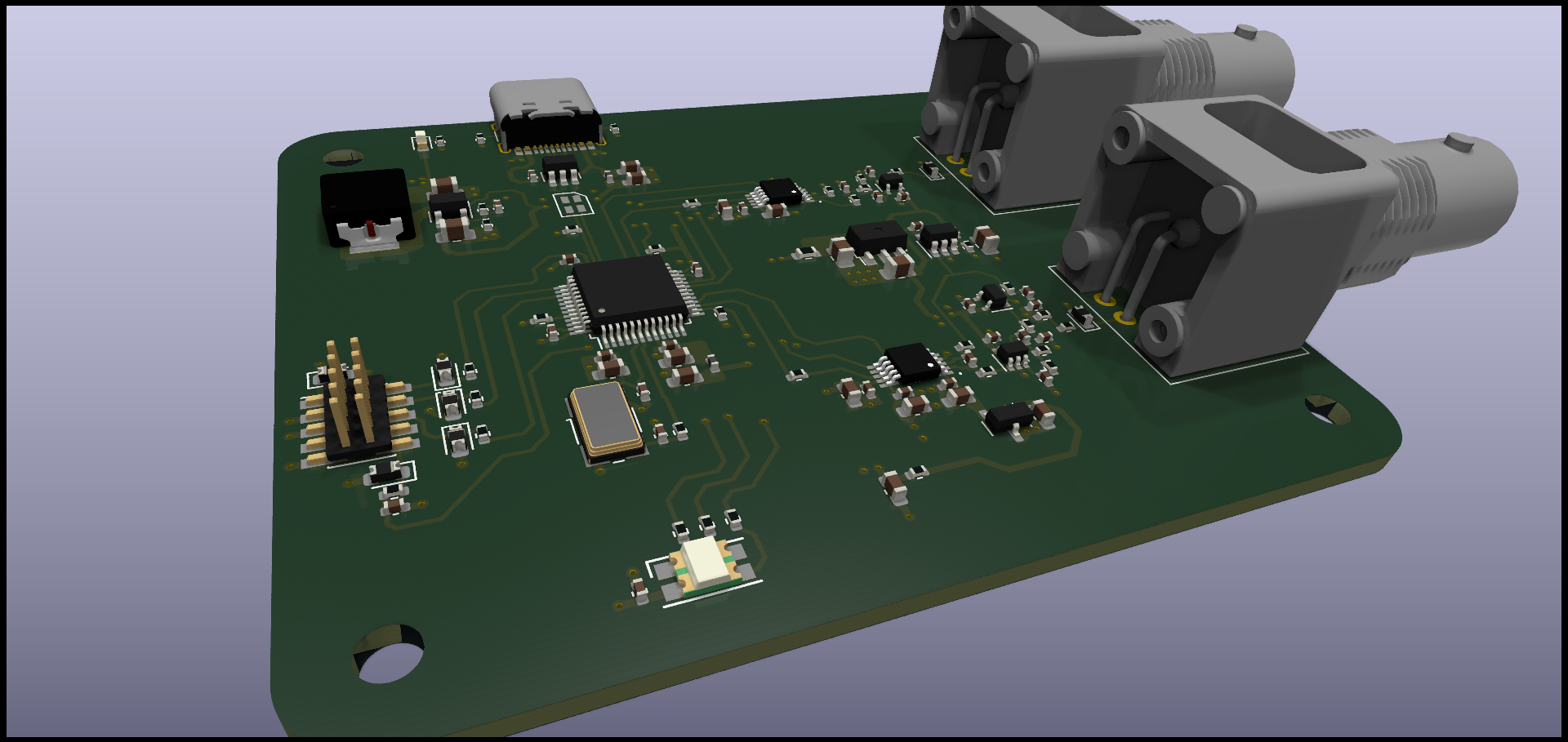
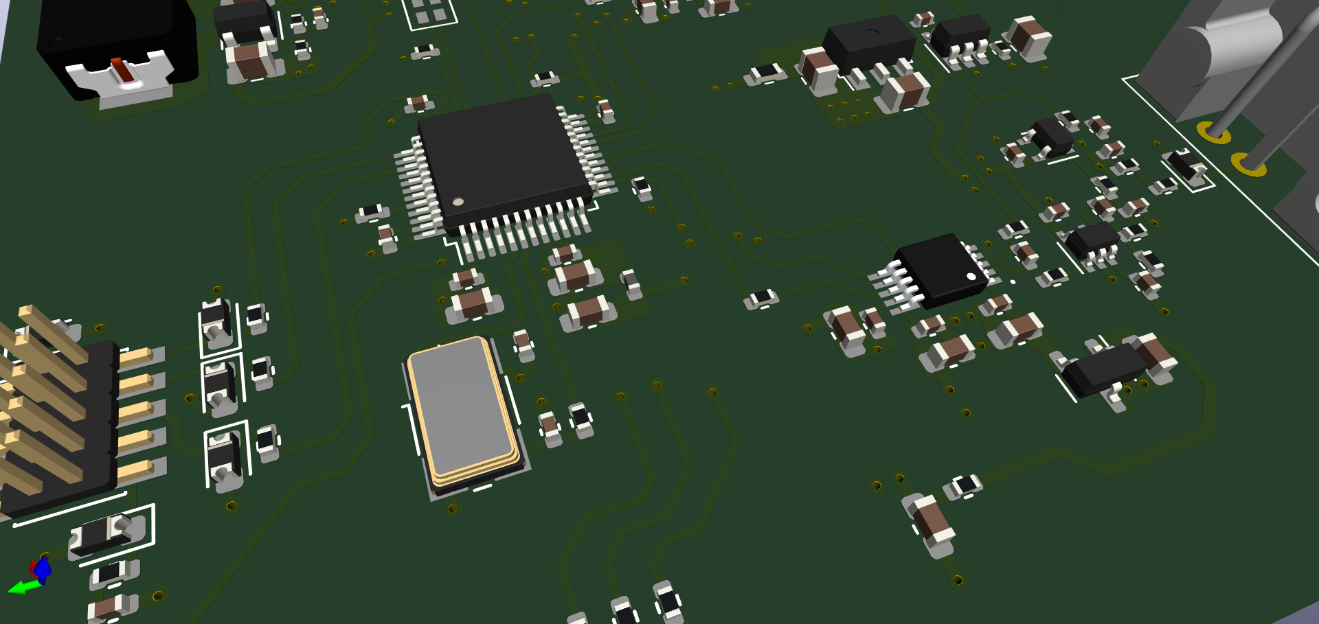
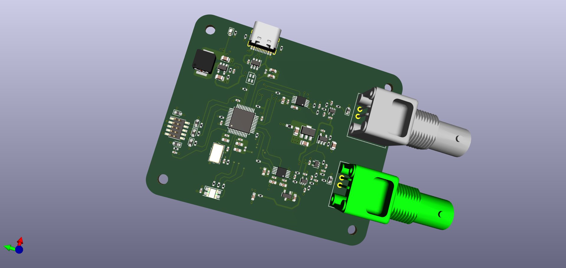
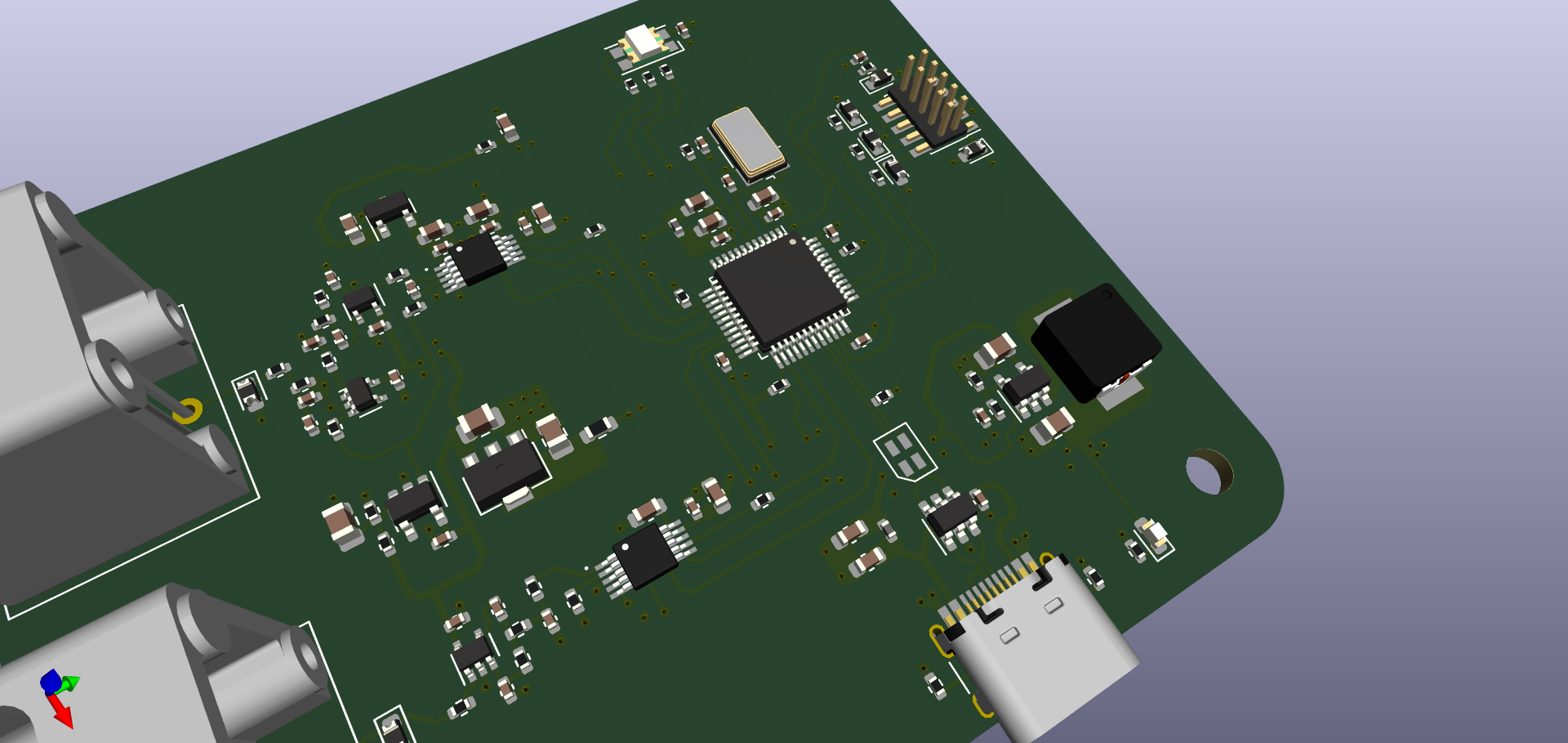
What this board does
This is a software-defined mixed-signal instrument. Rather than buying a separate function generator and oscilloscope, it implements both in one compact PCB using the STM32's on-chip ADC and DAC.
The BNC connectors are the standard lab-instrument interface — they let the board connect directly to other instruments (scopes, generators, DUTs) over 50 Ω coax, so it drops into a professional bench setup.
Schematic architecture — four sub-sheets
The schematic is split into four hierarchical sub-sheets in KiCad, each owning one functional block. It keeps every sheet focused and lets the top level show the system architecture without drowning in component detail.
⚡ Power — USB regulation
The board is powered entirely from the USB Micro B connector (5 V at up to 500 mA on VBUS), stepped down to 3.3 V for the MCU and signal chain.
📊 ADC — signal input & conditioning
Raw signals at a BNC input can't go straight into the MCU's ADC — they need conditioning first:
| Stage | Component | Why it's needed |
|---|---|---|
| Input protection | Clamping diodes / TVS | Keeps the pin within 0–3.3 V; the ADC input is only rated 0 to VDDA, and over-voltage permanently damages the MCU. |
| Anti-aliasing filter | RC low-pass | Nyquist requires removing everything above half the sample rate before sampling, or it aliases into the passband as false low-frequency signals. |
| DC bias / offset | Divider or op-amp | The ADC measures 0–3.3 V, so an AC signal centred on 0 V must be shifted up to VDDA/2 (1.65 V) or its negative half is clamped. |
🎵 DAC — signal generation & output
The STM32's internal DAC has a multi-kΩ output impedance. Drive a 50 Ω cable/load directly and the signal nearly vanishes in the divider, so a buffer amplifier sits between the DAC and the BNC output.
The DAC output is also a stepped (zero-order-hold) waveform, so a reconstruction low-pass filter at or below f_s/2 smooths the steps into a clean analog signal instead of a high-harmonic staircase.
🖥️ MCU — STM32 core and USB
The STM32, its support components (crystal, decoupling, reset), and the USB interface. The MCU's DMA controller is key here: it lets the ADC fill a buffer and the DAC drain a buffer without CPU involvement, so the CPU can run FFTs, USB and a display while DMA streams the real-time ADC/DAC at a precise, timer-clocked sample rate.
Mixed-signal design principles applied
A mixed-signal PCB carries both noisy digital circuits (MCU, USB, oscillators) and sensitive analog ones (ADC/DAC paths, op-amp buffers, BNC connectors). The whole challenge is keeping the digital noise out of the analog path.
🌐 Ground-plane strategy — the most critical decision
I used a single solid ground plane with careful placement, rather than split analog/digital planes joined at a star point:
- Split planes (star ground) stop digital return currents crossing the analog ground, but the seam creates impedance discontinuities and the star point is easy to get wrong.
- One solid plane with analog components physically separated from digital ones lets return currents — which at high frequency flow directly under their trace — stay in their own regions naturally. This is the Henry-Ott / modern-SI recommendation, and what I used.
📡 BNC connector — the 50 Ω standard
Key learnings
- Mixed-signal partitioning — where digital noise enters the analog path and how ground strategy controls it.
- Anti-aliasing filter design from the sample rate, and the Nyquist/aliasing intuition behind it.
- DAC output buffering — why output impedance matters and how an op-amp follower fixes loading.
- BNC selection and the meaning of 50 Ω impedance matching in bench instrumentation.
- Hierarchical schematic design in KiCad — splitting a complex design into clean functional sub-sheets.
- USB CDC on STM32 and DMA-driven ADC/DAC for precise, CPU-independent sample timing.