STM32F405 Development Board with Switching Supply
A compact 4-layer development board around the STM32F405RGT6: an on-board 12V→3.3V synchronous buck converter, USB OTG FS, SWD debug, I²C and UART breakouts, and reverse-polarity protection — designed from scratch in KiCad to understand every decision from the datasheet up.
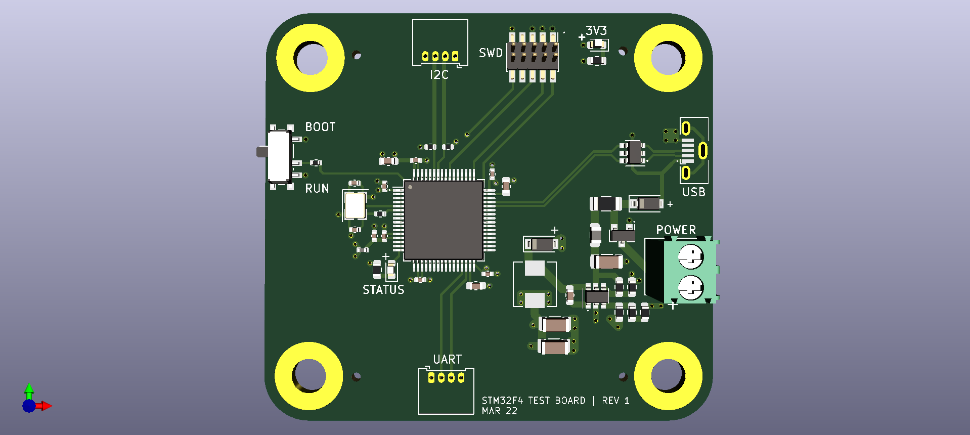
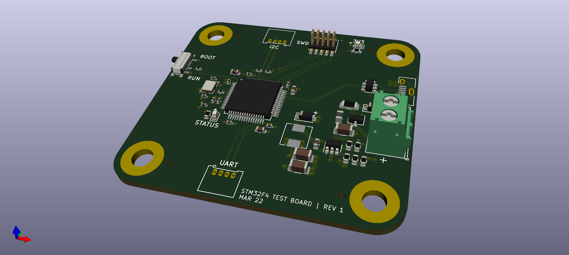
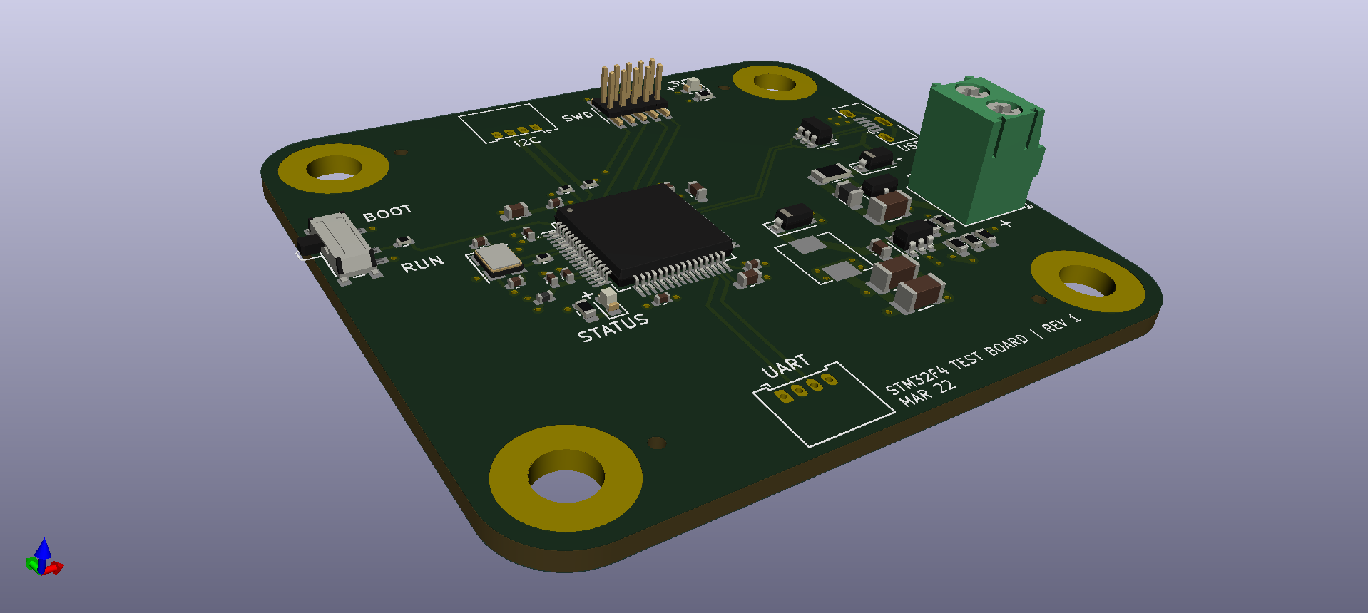
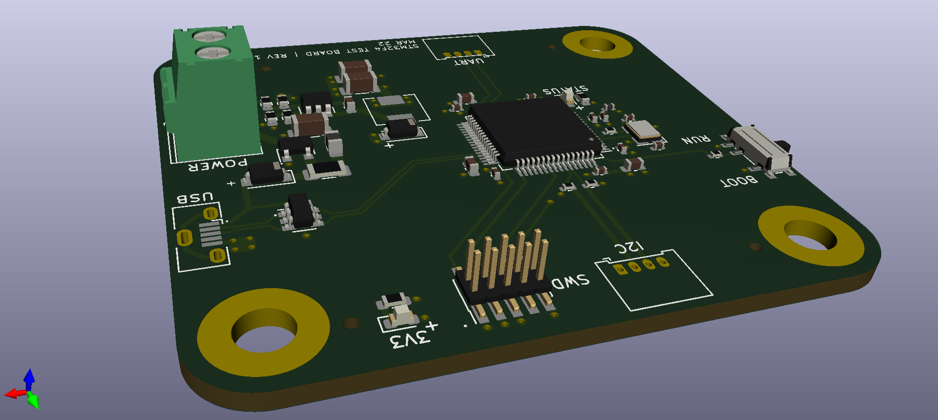
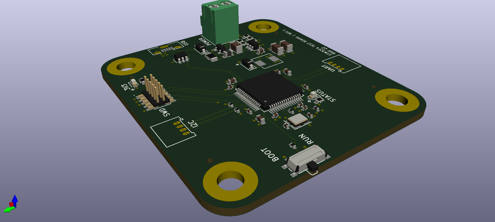
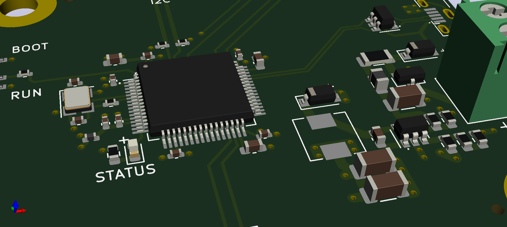
Board renders
3D renders straight from KiCad, showing the populated board from a few angles.
Why this board exists
Most people learn embedded firmware on an off-the-shelf Nucleo or Discovery board — and the catch is you don't control the hardware: which peripherals are exposed, what power topology feeds the MCU, how debug is wired. Building my own forced me to understand every design decision from the datasheet level.
It's a minimal but complete STM32 platform: 12 V in via a screw terminal, stepped down to 3.3 V by a switching regulator, with USB, SWD, I²C and UART broken out. The idea was to reuse it as the compute core in future projects running off a 12 V rail.
Power subsystem — deep dive
The power section is the most involved part: 12 V in to a clean, stable 3.3 V rail.
🛡️ Reverse-polarity protection — P-channel MOSFET (Q1)
The first thing 12 V hits is a P-channel MOSFET (AO3401A) acting as a reverse-polarity switch. Without it, hooking the supply up backwards would instantly destroy every chip on the board.
🔌 Fuse (250 mA) and ferrite bead (600 Ω @ 600 MHz)
A 250 mA fuse in series is the sacrificial element — a board short blows it open and protects the supply (normal draw is ~100–150 mA, so there's margin). After it, a ferrite bead behaves as a frequency-dependent resistor: near-zero impedance at DC (doesn't affect power delivery), high impedance at MHz (keeps switching noise from propagating back up the input cable).
⚡ Buck converter (NP2399DJ)
The heart of the power section is a fixed-frequency synchronous step-down converter that turns 12 V into a regulated 3.3 V.
An R1/R2 divider on the EN pin gives undervoltage lockout (the converter only starts once the input is high enough), and a feedback resistor network programs the output: the internal error amp compares the FB pin to a 0.8 V reference, so
| Component | Value | Function |
|---|---|---|
| L1 | 10 µH | Main inductor — larger L means smaller ripple but bigger and slower. |
| D2 | B5819W Schottky | Catch/freewheeling diode — low forward drop (~0.3 V) to cut conduction loss. |
| C2, C3 | 2× 10 µF | Output filter — two in parallel halve ESR/ESL and add bulk for transients. |
| C1 | 10 µF | Input bulk — absorbs the pulsed input current so the input rail doesn't droop. |
| D3 | LED | Power-good indicator — lights when 3.3 V is present. |
Microcontroller — STM32F405RGT6
A Cortex-M4F up to 168 MHz with 1 MB Flash and 192 KB SRAM — chosen over the usual F103 because it has native USB OTG FS and a hardware FPU for any DSP work.
🔮 16 MHz HSE crystal
The internal RC oscillator is ±1% — fine for GPIO, not for USB, which needs the timing source within ±0.25%. The external crystal (~±20 ppm) is required for USB. Two 12 pF load caps in the Pierce configuration set the load:
A 47 Ω series resistor on OSC_OUT limits drive current to prevent overdriving the crystal into an overtone mode (per ST's AN2867).
🔋 VCAP capacitors (2.2 µF each)
The F405 has an internal 1.2 V core regulator that needs two external filter caps to stay stable.
📦 Decoupling and the analog domain
The F405 has several VDD pins plus a separate VDDA — each gets its own decoupling cap right at the pin: a 4.7 µF bulk reservoir plus 100 nF high-frequency caps per VDD.
The VDDA pin is separated from digital VDD by a ferrite bead and filtered with 10 nF + 1 µF, creating an isolated analog domain so the ADC doesn't read noise from CPU fetches and USB.
🔄 BOOT0 and reset
The MCU picks its boot source from BOOT0 at power-on:
| BOOT0 | Boot source | Use |
|---|---|---|
LOW | User Flash | Normal — runs firmware from internal Flash. |
HIGH | System bootloader | DFU mode — flash over USB with no programmer. |
A slide switch selects the mode (10 kΩ pulls BOOT0 low by default), and a reset button re-reads it.
USB OTG FS
The F405's built-in OTG controller can act as host or device on one Micro B port. ESD is the real hazard here.
Debug interfaces
🔧 SWD (10-pin)
ARM's 2-wire debug — SWDIO (data) and SWCLK (clock), plus optional SWO trace and NRST.
📟 UART & I²C breakouts
USART3 on a 4-pin header for printf/console over a USB-UART dongle (keeping the OTG port free), and I²C1 broken out for displays, IMUs, sensors and RTCs on a shared 2-wire bus.
PCB layout — 4-layer strategy
- L1 (top signal) — component pads and primary routing.
- L2 (ground plane) — solid GND: a tight return path for every L1 signal, low decoupling-loop inductance, and EMI shielding.
- L3 (power plane) — 3.3 V pour distributing power to every VDD without fat traces on signal layers.
- L4 (bottom signal) — extra routing for connectors and power parts.
Placement follows functional zones: power on the right (short high-current paths kept away from the MCU), the STM32 and its decoupling/crystal in the centre, interface headers around the perimeter, and the BOOT/RUN switches on the left edge for easy bring-up.
Key learnings
- The full KiCad workflow end to end: schematic → PCB → Gerber → 3D render.
- Reading IC datasheets to extract the application circuit, instead of copying a reference.
- Buck feedback-network design from first principles — resistor values from the target output.
- Analog/digital power-domain separation and how a ferrite bead implements it.
- Crystal load-cap calculation and the role of the series drive resistor.
- USB ESD-suppressor placement — within ~1 mm of the connector.
- 4-layer stackup design and why a solid ground plane is non-negotiable with USB or switching power.